Rampage
The next generation of hardware from 3dfx that would have vaulted the company into the performance lead.
There is a lot of information floating around about the 3dfx Rampage chip, I'll try to hit some highlights while not getting bogged down into too much detail.
Rampage: A new chip architecture from 3dfx that looked to raise the bar in the graphics industry like Voodoo Graphics did in 1995. The chip was actually to be used in a series of boards much like the VSA-100 was used in 4500, 5500 and 6000. Moving away from the Voodoo name, the boards were to be called SPECTER 1000, 2000, 3000. A board with a single Rampage chip was called SPECTER 1000. If a board had a single Rampage chip and a Sage transformation and lighting unit it would have been a SPECTER 2000. A board with TWO Rampages and ONE Sage would have been a SPECTER 3000.
The price breakdown and board configuration was *suppose* to be this-
1 Rampage chip w/64MB $200
USD
1 Rampage/1 Sage w/64MB $300 USD
2 Rampage/1 Sage w/128MB $500 USD
Note- The flagship product Specter 3000 would have been a killer piece of hardware for the time frame. 2 Rampage chips in SLI mode with Sage combined with DDR ram would have had 10.2 GB/S bandwidth with a fillrate of 1600-2000Mpixels/S.
To give you a point of reference Nvidia didn't have anything matching these performance specs till some Geforce 4 models were released years later.
Rumor has it the Rampage chip was in development as far back as 1997 and was delayed by feature creep and members of the team being drawn off by other projects. I'll try to look into those rumors but contacting a few friends of mine and see if we can come up with some hard information. You can download an internal Rampage Power Point file here dated April 1999 but the file indicates it was modified October of 2000 so chances are some of the information is suspect.
How many Rampage boards were there? By my estimates and statements made by former engineers the number rests at twenty total. Of those, ten are A0 revision and the other ten are A1 revision. What is known is the A1 boards were pretty solid and engineers were busy hammering away getting the boards running correct right up to the day they were laid off.
Could Rampage have saved the company? Without knowing all the facts it is tough to say, but it would have been another 6 months before the first SPECTER boards started showing up on the shelves with only the Daytona and the older Napalm chips to shoulder the burden till then. The Specter family of boards was very powerful and would have outperformed any other current graphics solutions by a wide margin.
While 3dfx was starting to cut their costs, sell off the STB manufacturing plant and go back being just a chip provider it was too late.
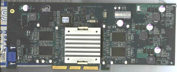
Yes, I own the board shown at the bottom of the page and it works just fine.
Here are some Rampage specs that have been provided to me:
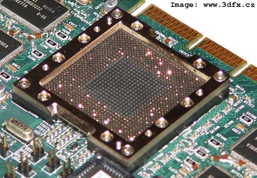
Rampage is based on the 0.18micron process with 25 Million transistors and the core would have ran at 200-250Mhz depending on yields and stability. Each chip sported four pixel pipelines with one TMU assigned to each pipe. Its fillrate hence would have being 800-1000MegaPixels/Texels. Although there's only 1 TMU per pipe, the chip can out match the NV20 in Multi-texturing as it can apply 8 textures in a single pass. This is done using Rampage's texture computer and its unique "loopback" function.
Rampage rasteriser:
· Rampage Texture computer
with "loopback"
· 3dfx M-Buffer (Multi-Sample Buffer)
· 2x/4x RGMS Full Scene AntiAlising
· Up to 128Tap anisotropic filtering
· 52bit Internal Color rendering precision / 0 - 16.0 Color luminosity
range
· FXT1/DXT1 Texture compression · 3D textures support
· True PhotoShop filter effects in hardware
· Non-Photorealistic rendering
· Cube Environment Maps/EMBM/Dot3 BM
· YUV Texture formats
· 1/2/4 chip scalability
· Fully programmable DirectX8 1.1compiant Pixel Shaders with additional
features (DX9)
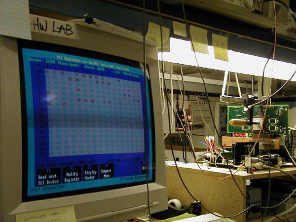
Quote from 3dfx engineer: "This is Rampage, and that is my debug station. What you are looking at is a BGA socket and not a strange heatsink.
Quote from 3dfx engineer: "The socket had contact problems, so you see a C-clamp on top. The PCI ID you see is 3DFX 121Ah. The program is PCI.EXE, it is old so it did not have an entry for 3DFX ID in it. The riser was there so I could see if the card responded to AGP cycles. I woke the first one up this way and made sure we could talk to it. The card is in multimedia mode so another VGA card can be used to monitor the system. Simple first steps in debug."
"The reason it looks so weird is that THOSE ARE BRING UP BOARDS!! (Note the AGP riser card for testing bus timings) It is not indicative of the final board at all."
Quotes from 3dfx engineer:
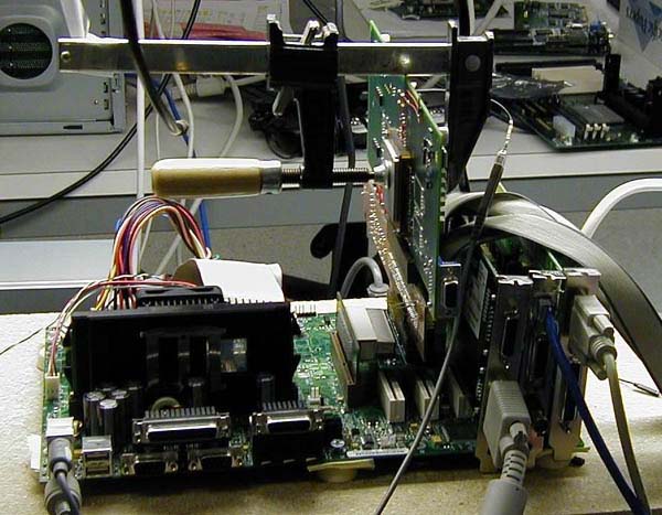
"It is a rampage bring up REV-A0 board that only 10 were made. It had serious problems as you can see. It was rushed through design a little too fast and a lot of corners were cut to get that P.O.S. you see in the picture (not my decision - it was upper managements). only 2 boards ever worked of the REV-A0. It lived for approx. 2 weeks until the REV-A1 design was done. There were about 10 REV-A1's that we debugged and it ran fine. all the problems you see (the clamp etc.) were fixed in the A1 revision. The REV-A1 boards screamed. We were laid off on Friday we had debugged that board till Thursday night. It ran Quake3, It would have been a real threat to Nvidia due to cost and performance. We hit 250 Mhz DDR"
This section came from the old Slacker Central website and is reported to be from 3dfx intranet engineering logs. I'm trying to find out if there is any more information like this as it really gives us a unique insight as to what was going on at the time.
11/15/00 5:27 PM Stuffed Rampage bringup board being reworked. Rework is fixing power supply connection issues. Estimated time to completion "a while". Probably about 8 hours to rework and verify.
11/16/00 3:20 PM With a lot of work, the board engineers have been able to rework one bringup board. We currently have applied power to the first Rampage chip. Bringup of the chip is underway. We are continuing to work on a clean up of the database for the first bringup board.
11/16/00 8:45 PM The engineers have been working thorough intermittent contact problems in the socket area this evening. Progress has been slow because the chip responds for awhile then stops responding.
11/17/00 5:35 PM Rampage bringup has made little progress today. This morning the engineers were able to read a few registers before the board stopped working. During the day the debug effort continued to point to socket issues. Therefore, we are currently mounting a chip down on the board in an attempt to make more progress. In addition, we are completing three more of the initial bringup boards. We are planning on reworking at least one more board. The respin of the initial bringup board is underway. The current target for completion of the respin is Saturday about noon. We will not attempt to fab more boards until we have high confidence in the database. We will quick turn 3 to 5 boards to make sure the board is correct before building any larger quantity. The second bringup board is continuing to make progress in layout including incorporating the new chip model. This board may be ready for fab by the middle of next week.
11/22/00 Here is what has happened in the last 24 hours. The new version of the initial bringup board bare fab arrive this morning and was sent to the assembly house. We should get new stuffed boards back Wednesday afternoon. The socket fits well on the new board. Our next big push needs to be to get the memory working and stable. We got the DAC's aPwr and GND hooked up, and now we get relatively clean and stable garbage on the video monitor. We've been able to flash and read the ROM reliably, although there may be work left in the 32K-64K address range. We're bringing up our second board with Joe Minacapelli's patented socket holding device, and other rework to ensure stability. PCI clock insertion workaround and PCI clock PLL fixes are underway. We've been able to do a 2d blit, but because the memory system's not stable, it didn't look perfect, but it did look like it did a blit. We tried bringing up the windows driver with Rampage as the secondary device, and it recognized the card, and allowed us to debug some of the modeset code.
11/29/00 Rampage is running but there are some stupid bugs. The DAC output is reversed ... high is low and low is high which turns out to be rather sucky since displaying is difficult. Looking at a dongle to invert the inverted output. Flash ROM bug where part can't be written... Fixes for both are possible in metal layers. 5 boards are operational.
11/30/00 DAC output ‘dongle’ fitted. Rampage running D3D applications. And soon after that the D3D DX8 demos were running and Quake3 debugging in a window (which we’ve also seen pictures of).
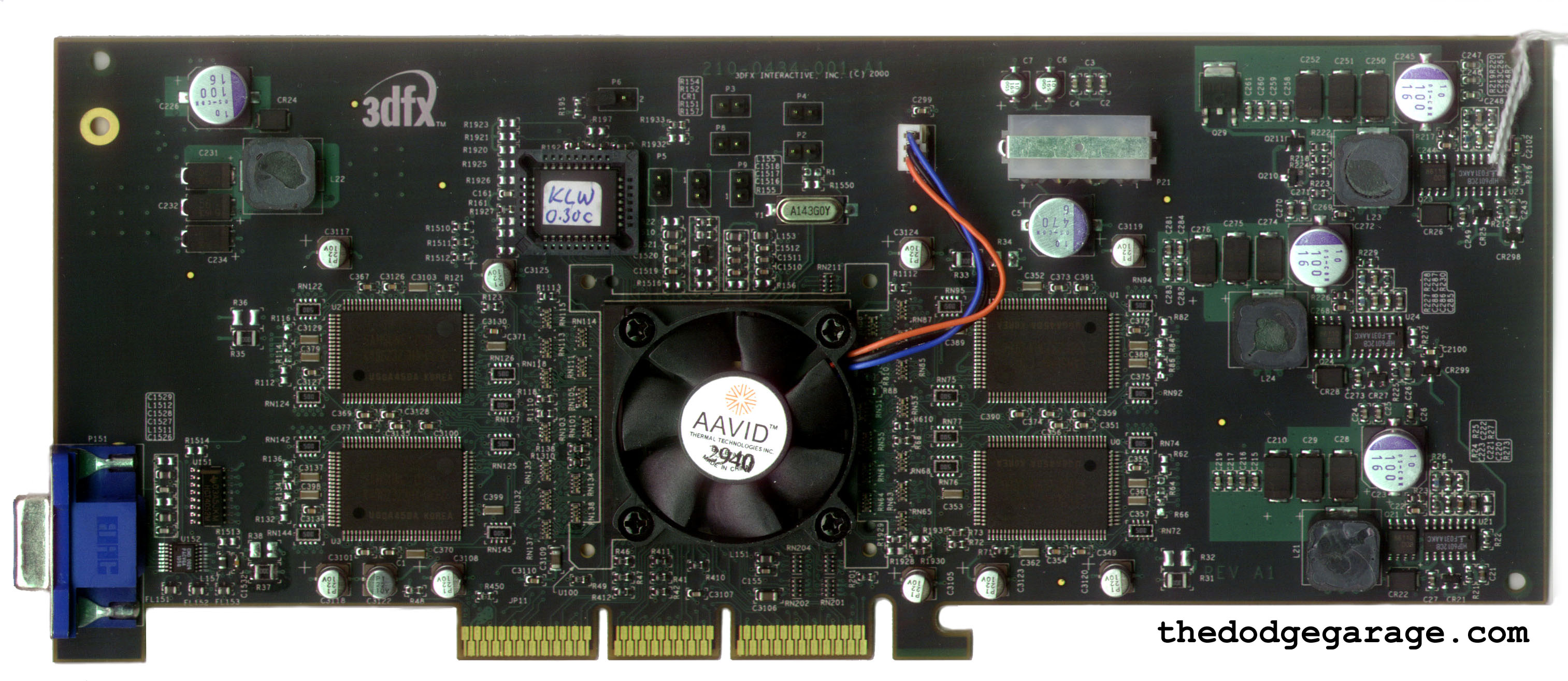
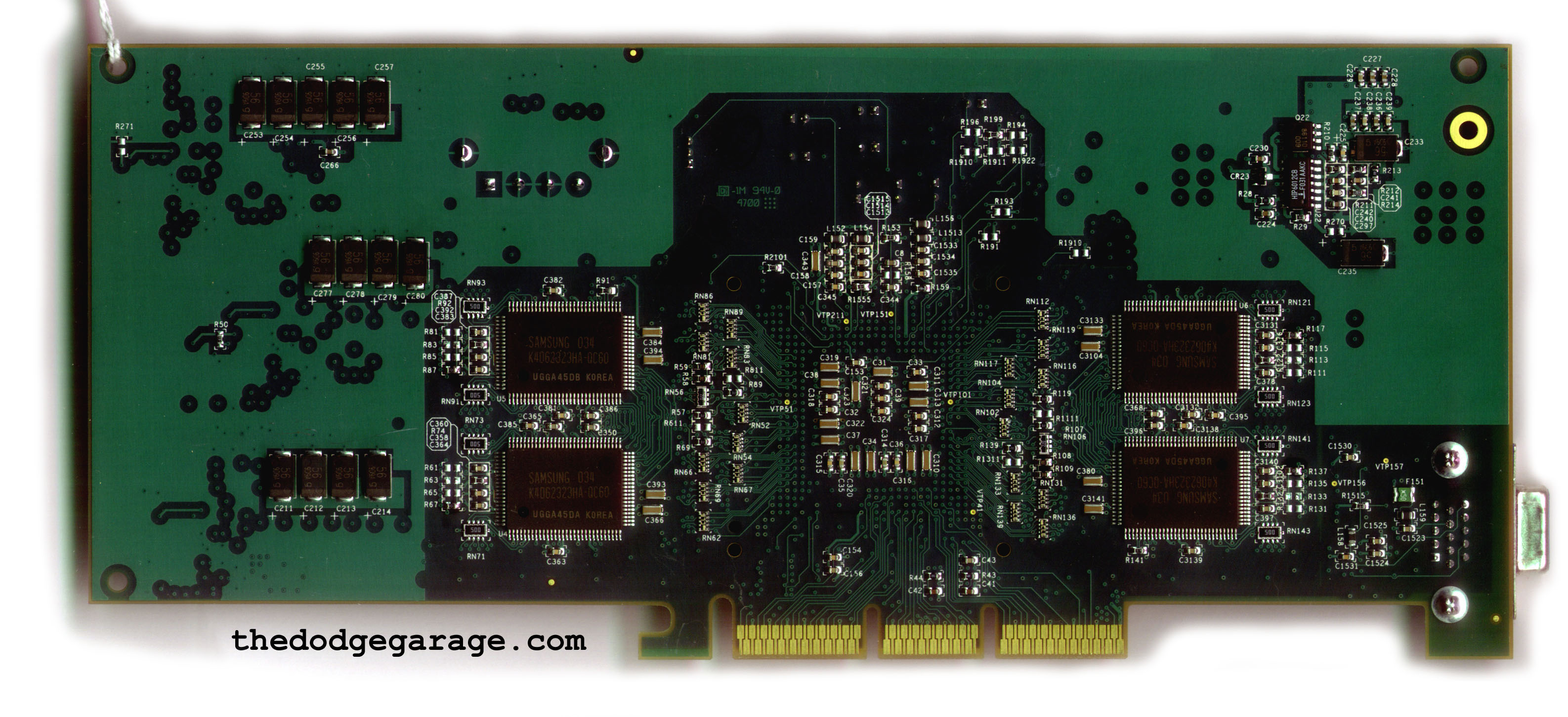
Front and rear views, click for larger image in new window.
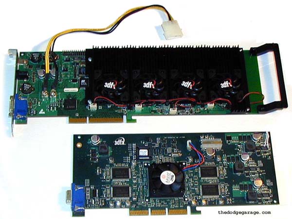
Shown in comparison to my V5-6000 with prototype cooler assembly.
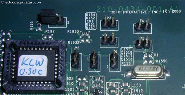
Close up of the BIOS chip, some jumpers and PCB number with revision.
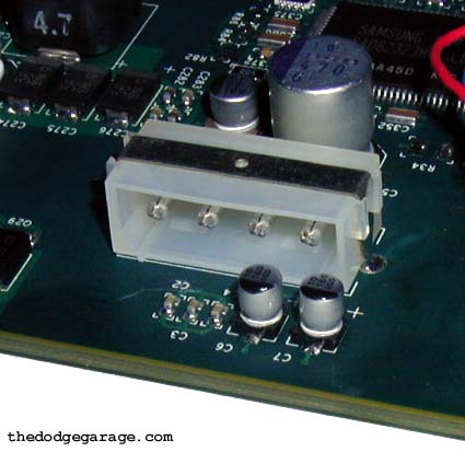
Check this out: The Molex connector for extra power is being blocked by two capacitors! The reason for the Molex connector was that since the chip was 100% modeled in software it was unknown if the AGP connector could provide enough power.
As it turned out the extra power was not required which is just as well since a snafu in the PCB layout ended up blocking the connector anyway.
NOTE: I'm told by an engineer that hooking power to the connector will cause something very unpleasant to happen to the board. So if you come across a Rampage board, don't try plugging power in here, the board runs just fine without it.
Close up of a DDR ram module, total of eight.
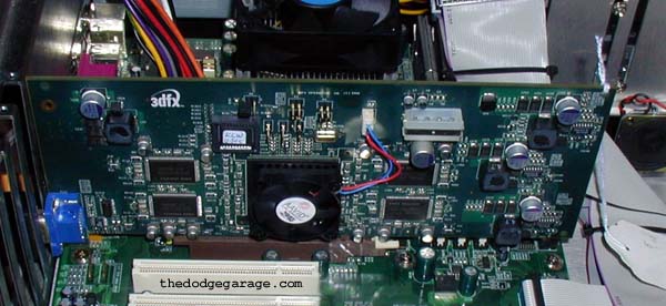
Installed in the Q3D-V6K box with KT-333 chipset Epox motherboard.
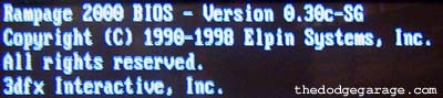
Board information on boot up (which indicates it is 32 MB card)
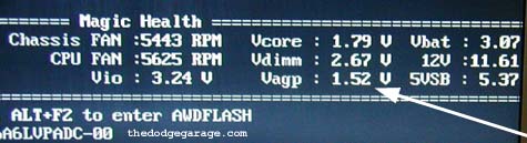
1.5 AGP volts not 3.3 AGP volts like earlier 3dfx AGP boards.
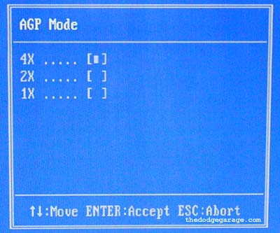
True 4x AGP support.
![]()